The thin wafer market plays a pivotal role in driving innovation within the semiconductor industry. A thin wafer is a semiconductor substrate reduced to a minimal thickness, typically less than 200 micrometers, enabling advanced packaging solutions for electronic devices. As demand for compact and high-performance consumer electronics rises, thin wafers provide the necessary foundation for creating smaller, lighter, and more efficient devices. The market is expanding rapidly, driven by increasing applications in smartphones, wearable technology, automotive electronics, and power devices, contributing to enhanced processing power and energy efficiency.
Thin wafers are essential for 3D integration, a technology that allows stacking multiple wafers or chips vertically, leading to more powerful semiconductor devices. These wafers also enable advancements in micro-electromechanical systems (MEMS), photovoltaic cells, and advanced LED packaging, ensuring their relevance in key sectors.
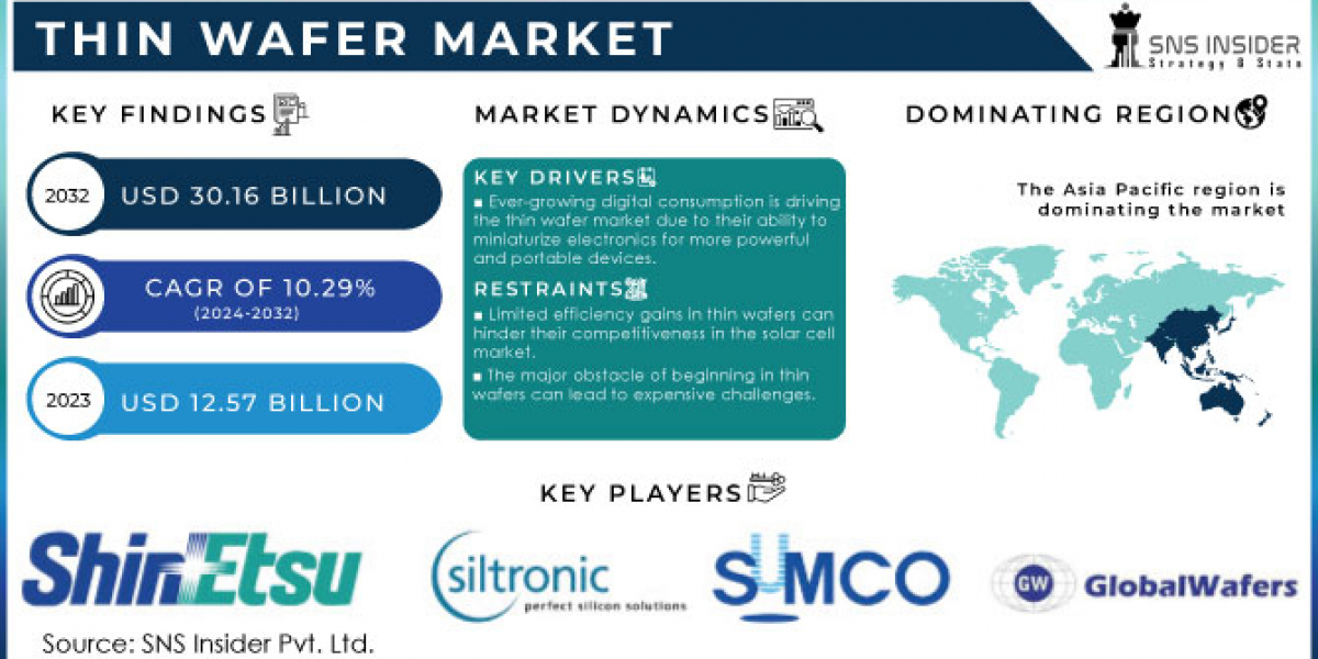
The Thin Wafer Market size was valued at USD 12.57 Billion in 2023 & expects good growth by reaching USD 30.16 billion till the end of 2032 at a CAGR of about 10.29 % during the forecast period 2024-2032.
Future Scope
The thin wafer market is expected to grow exponentially as the semiconductor industry seeks new ways to meet the demands of high-performance computing and data storage. The transition towards 5G, the Internet of Things (IoT), and artificial intelligence (AI) will further drive the adoption of thin wafers in next-generation technologies. With ongoing developments in wafer thinning processes, including chemical mechanical planarization (CMP) and temporary bonding methods, manufacturers will continue to achieve thinner substrates with higher yield rates, enhancing overall device performance.
As 3D packaging and system-on-chip (SoC) designs gain prominence, thin wafers will become increasingly critical in enabling high-density circuits, reducing power consumption, and improving thermal management. The growing demand for flexible electronics and advancements in bendable and foldable display technologies will also fuel market expansion, offering new opportunities for thin wafer integration.
Trends
One of the key trends in the thin wafer market is the shift towards advanced packaging techniques such as wafer-level packaging (WLP) and through-silicon vias (TSV). These methods enhance the performance of electronic devices by allowing more compact designs and better thermal dissipation. Another trend is the increasing use of thin wafers in power devices for energy-efficient systems in automotive and industrial applications, driven by the demand for electric vehicles (EVs) and renewable energy solutions.
The rise of compound semiconductors, such as gallium nitride (GaN) and silicon carbide (SiC), is also reshaping the thin wafer landscape. These materials offer superior performance in high-frequency, high-voltage applications, making them ideal for power electronics and optoelectronic devices. Additionally, manufacturers are investing in automation technologies to optimize the wafer thinning process, reducing production costs and improving output quality.
Applications
Thin wafers are widely used in various applications across multiple industries. In consumer electronics, they are essential for the production of smartphones, tablets, and wearable devices, providing the foundation for compact, lightweight designs with high processing power. The automotive industry leverages thin wafers for sensors, advanced driver assistance systems (ADAS), and in-vehicle infotainment systems, supporting the development of autonomous and electric vehicles.
In the energy sector, thin wafers are used in power semiconductors to improve energy conversion efficiency in renewable energy systems such as solar panels and wind turbines. Additionally, they play a critical role in MEMS technology, which is employed in sensors, actuators, and medical devices, enabling precise measurements and control in various applications.
Solutions and Services
Several leading companies in the semiconductor industry offer specialized solutions and services for thin wafer manufacturing. These include advanced wafer thinning, dicing, and bonding technologies that ensure the structural integrity and performance of thin wafers. Key service providers offer expertise in wafer-level packaging, TSV, and flip-chip bonding, optimizing the production process for high-volume manufacturing.
Additionally, manufacturers are focusing on developing innovative wafer handling techniques to prevent warping or damage during the thinning process. Solutions also include the development of materials for temporary bonding and debonding, which allow for easier processing and handling of thin wafers. These services are tailored to meet the specific needs of industries such as consumer electronics, automotive, telecommunications, and renewable energy.
Key Points
- Thin wafers are essential for enabling compact, high-performance semiconductor devices.
- Growing demand for 5G, AI, IoT, and advanced computing is driving thin wafer market expansion.
- Key trends include wafer-level packaging (WLP), through-silicon vias (TSV), and the rise of compound semiconductors.
- Applications span across consumer electronics, automotive, energy, and MEMS technologies.
- Leading companies provide solutions in wafer thinning, bonding, and packaging to meet industry requirements.
Read More Details: https://www.snsinsider.com/reports/thin-wafer-market-4376
Contact Us:
Akash Anand — Head of Business Development & Strategy
Email: info@snsinsider.com
Phone: +1–415–230–0044 (US) | +91–7798602273 (IND)